Using PlatformIO with a custom board based on STM32F427VGT6 mcu

I’m a newcomer to PlatformIO, have used it for several simple ESP32 projects, and I love it!

Now I’m embarking on a more serious project – writing an app that will run on a custom board based on the STM32F427VGT6 mcu. This same board was previously programmed by someone else using VisualGDB, but I want to use PlatformIO,

I’m struggling a bit getting started, and would appreciate any and all assistance.

Is anyone else out there using the STM32F427VGT6 with PlatformIO?

Thanks!
~neurodancer

There are only two board definitions close the the STM32F427VG: Both use a F427VI.

https://github.com/search?q=repo%3Aplatformio%2Fplatform-ststm32+STM32F427V&type=code

But it’s also possible to create a new board definition for the STM32F427VGT6, based on e.g. this one, and use the Arduino framework with it (as provided e.g. by Arduino_Core_STM32). For this special case, the Arduino framework doesn’t supply the linkerscript (ldscript.ld), so we have to supply our own.

The board definition is by default setup to expect an ST-Link upload and debugging tool, but you can change it to any of the other supported ones as is documented (here, here).

1 Like

Hey Maximilian,

Thank you very much for your detailed response to my request for help.

I finally had time today to read it in detail, and then I cloned the repo that you prepared. When I built the project everything worked perfectly the first time!

You have saved me a great deal of time and frustration. I am very grateful.

Dude, you’re awesome!

My project is progressing, but now that I’ve added numerous files to it I have encountered the following error while building my project:

Linking .pio/build/genericSTM32F427VG/firmware.elf
/Users/myname/.platformio/packages/toolchain-gccarmnoneeabi@1.70201.0/bin/../lib/gcc/arm-none-eabi/7.2.1/../../../../arm-none-eabi/bin/ld: invalid length for memory region RAM

Since I’m a neophyte PIO user I’m not sure where I need to look in order to fix this. I’ve tried making a change to my board definition file and also to the platform.ini file, but so far have not been able to fix the error.

Here is my board file:

{
    "build": {
      "core": "stm32",
      "cpu": "cortex-m4",
      "extra_flags": "-DSTM32F4 -DSTM32F427_437xx -DSTM32F427xx -DARDUINO_GENERIC_F427VGTX",
      "f_cpu": "180000000L",
      "mcu": "stm32f427vgt6",
      "product_line": "STM32F427xx",
      "variant": "STM32F4xx/F427V(G-I)T_F429V(E-G-I)T_F437V(G-I)T_F439V(G-I)T"
    },
    "debug": {
      "default_tools": [
        "stlink"
      ],
      "jlink_device": "STM32F427VG",
      "onboard_tools": [
        "stlink"
      ],
      "openocd_target": "stm32f4x",
      "svd_path": "STM32F427x.svd"
    },
    "frameworks": [
      "arduino",
      "cmsis",
      "spl",
      "stm32cube",
      "libopencm3"
    ],
    "name": "Generic STM32STM32F427VG",
    "upload": {
      "maximum_ram_size": 114688,
      "427_ram_size": 262144,
      "maximum_size": 1048576,
      "protocol": "blackmagic",
      "protocols": [
        "jlink",
        "cmsis-dap",
        "stlink",
        "blackmagic"
      ]
    },
    "url": "https://www.st.com/en/microcontrollers-microprocessors/stm32f427vg.html",
    "vendor": "Armstrap"
  }

And here is my platform.ini file:

; PlatformIO Project Configuration File
;
[env:genericSTM32F427VG]
platform = ststm32
board = genericSTM32F427VG 
board_build.ldscript = ldscript.ld
upload_protocol = stlink
upload_port = /dev/ttyUSB0
build_flags = -I/lib/BaseWin
maximum_ram_size = 262144

Any and all suggestions would be greatly appreciated!

~neurodancer

So what’s the content of the ldscript.ld?

Setting maximum_ram_size = 262144 doesn’t work like that. If anything, you would need to affect

board_upload.maximum_ram_size = 262144

but, since your board JSON file already has that, that it not necessary. Also setting "427_ram_size": 262144 in the Json file has no effect.

Here’s the ldscript.ld file:

/**
 ******************************************************************************
 * @file      LinkerScript.ld
 * @author    Auto-generated by STM32CubeIDE
 * @brief     Linker script for STM32F429ZITx/STM32F439ZITx Device from STM32F4 series
 *                      1024Kbytes FLASH
 *                      64Kbytes CCMRAM
 *                      192Kbytes RAM
 *
 *            Set heap size, stack size and stack location according
 *            to application requirements.
 *
 *            Set memory bank area and size if external memory is used
 ******************************************************************************
 * @attention
 *
 * <h2><center>&copy; Copyright (c) 2020 STMicroelectronics.
 * All rights reserved.</center></h2>
 *
 * This software component is licensed by ST under BSD 3-Clause license,
 * the "License"; You may not use this file except in compliance with the
 * License. You may obtain a copy of the License at:
 *                        opensource.org/licenses/BSD-3-Clause
 *
 ******************************************************************************
 */

/* Entry Point */
ENTRY(Reset_Handler)

/* Highest address of the user mode stack */
_estack = ORIGIN(RAM) + LENGTH(RAM);	/* end of "RAM" Ram type memory */

_Min_Heap_Size = 0x200;	/* required amount of heap  */
_Min_Stack_Size = 0x400;	/* required amount of stack */

/* Memories definition */
MEMORY
{
  CCMRAM    (xrw)    : ORIGIN = 0x10000000,   LENGTH = 64K
  RAM    (xrw)    : ORIGIN = 0x20000000,   LENGTH = LD_MAX_DATA_SIZE
  FLASH    (rx)    : ORIGIN = 0x8000000 + LD_FLASH_OFFSET, LENGTH = LD_MAX_SIZE - LD_FLASH_OFFSET
}

/* Sections */
SECTIONS
{
  /* The startup code into "FLASH" Rom type memory */
  .isr_vector :
  {
    . = ALIGN(4);
    KEEP(*(.isr_vector)) /* Startup code */
    . = ALIGN(4);
  } >FLASH

  /* The program code and other data into "FLASH" Rom type memory */
  .text :
  {
    . = ALIGN(4);
    *(.text)           /* .text sections (code) */
    *(.text*)          /* .text* sections (code) */
    *(.glue_7)         /* glue arm to thumb code */
    *(.glue_7t)        /* glue thumb to arm code */
    *(.eh_frame)

    KEEP (*(.init))
    KEEP (*(.fini))

    . = ALIGN(4);
    _etext = .;        /* define a global symbols at end of code */
  } >FLASH

  /* Constant data into "FLASH" Rom type memory */
  .rodata :
  {
    . = ALIGN(4);
    *(.rodata)         /* .rodata sections (constants, strings, etc.) */
    *(.rodata*)        /* .rodata* sections (constants, strings, etc.) */
    . = ALIGN(4);
  } >FLASH

  .ARM.extab (READONLY) : {
    . = ALIGN(4);
    *(.ARM.extab* .gnu.linkonce.armextab.*)
    . = ALIGN(4);
  } >FLASH

  .ARM (READONLY) : {
    . = ALIGN(4);
    __exidx_start = .;
    *(.ARM.exidx*)
    __exidx_end = .;
    . = ALIGN(4);
  } >FLASH

  .preinit_array (READONLY) :
  {
    . = ALIGN(4);
    PROVIDE_HIDDEN (__preinit_array_start = .);
    KEEP (*(.preinit_array*))
    PROVIDE_HIDDEN (__preinit_array_end = .);
    . = ALIGN(4);
  } >FLASH

  .init_array (READONLY) :
  {
    . = ALIGN(4);
    PROVIDE_HIDDEN (__init_array_start = .);
    KEEP (*(SORT(.init_array.*)))
    KEEP (*(.init_array*))
    PROVIDE_HIDDEN (__init_array_end = .);
    . = ALIGN(4);
  } >FLASH

  .fini_array (READONLY) :
  {
    . = ALIGN(4);
    PROVIDE_HIDDEN (__fini_array_start = .);
    KEEP (*(SORT(.fini_array.*)))
    KEEP (*(.fini_array*))
    PROVIDE_HIDDEN (__fini_array_end = .);
    . = ALIGN(4);
  } >FLASH

  /* Used by the startup to initialize data */
  _sidata = LOADADDR(.data);

  /* Initialized data sections into "RAM" Ram type memory */
  .data :
  {
    . = ALIGN(4);
    _sdata = .;        /* create a global symbol at data start */
    *(.data)           /* .data sections */
    *(.data*)          /* .data* sections */
    *(.RamFunc)        /* .RamFunc sections */
    *(.RamFunc*)       /* .RamFunc* sections */

    . = ALIGN(4);
    _edata = .;        /* define a global symbol at data end */

  } >RAM AT> FLASH

  /* Uninitialized data section into "RAM" Ram type memory */
  . = ALIGN(4);
  .bss :
  {
    /* This is used by the startup in order to initialize the .bss section */
    _sbss = .;         /* define a global symbol at bss start */
    __bss_start__ = _sbss;
    *(.bss)
    *(.bss*)
    *(COMMON)

    . = ALIGN(4);
    _ebss = .;         /* define a global symbol at bss end */
    __bss_end__ = _ebss;
  } >RAM

  /* User_heap_stack section, used to check that there is enough "RAM" Ram  type memory left */
  ._user_heap_stack :
  {
    . = ALIGN(8);
    PROVIDE ( end = . );
    PROVIDE ( _end = . );
    . = . + _Min_Heap_Size;
    . = . + _Min_Stack_Size;
    . = ALIGN(8);
  } >RAM

  /* Remove information from the compiler libraries */
  /DISCARD/ :
  {
    libc.a ( * )
    libm.a ( * )
    libgcc.a ( * )
  }

  .ARM.attributes 0 : { *(.ARM.attributes) }
}

I was only using “427_ram_size” as a reminder, not expecting it to have any effect. I had previously used “maximum_ram_size”: 262144, but that did not fix the error, but thanks for pointing that out.

Since there is no framework = .. line in the platformio.ini you’ve shown, the linker variables LD_MAX_DATA_SIZE, LD_FLASH_OFFSET and LD_MAX_SIZE remain undefined. In the project above, which used framework = arduino, the builder script for the Arduino framework defined these variables, based on the information in the board file.

You have two options:

  • use advanced scripting to also add these flags in the env["LINKFLAGS"]
  • simply replace that section of the linker script with constant, static values. For example, assuming flash offset = 0 (no additional bootloader)
  RAM    (xrw)    : ORIGIN = 0x20000000,   LENGTH = 262144
  FLASH    (rx)    : ORIGIN = 0x8000000, LENGTH = 1048576

I used the constant, static approach for now, and that fixed the ram size error. TYVM.

Now I get this error further down in the ldscript.id file:

ldscript.ld:82: non constant or forward reference address expression for section .ARM.extab

I’ve looked at it for a couple of minutes, but I don’t understand enough about this build environment to see what’s wrong there.

Sounds like the same issue as in https://community.st.com/t5/stm32cubemx-mcus/clion-uses-arm-gcc-to-compile-code-generated-from-cubemx-file/m-p/653876/highlight/true#M27600 to me? Try just removing every (READONLY) in the file if the linker doesn’t support it.

Otherwise, upgrade your compiler to beyond GCC 10, for example per versions and docs through the platformio.ini

; Use GCC 14.2.1 to be able to use (READONLY) in linkerscript
platform_packages =
   toolchain-gccarmnoneeabi@~1.140201.0
; or ~1.120301.0

Per code, a framework = arduino project would use ~1.120301.0 (GCC 12.3.1) here. Without a framework, it seems to default to 1.70201.0 (GCC 7.2.1).

1 Like

Again, TYVM!

I removed all of the (READONLY)'s and the build finally reaches [SUCCESS]. I will look into upgrading my compiler to beyond GCC 10 as you suggest.

Your troubleshooting skills are truly LEET. Also, you are an awesome Teacher – your responses contain so much information that helps the rest of us learn.

:pray: :man_teacher:

~neurodancer

This project is a bare metal application that runs on an STM32F427VGT6 mcu. I inherited it from another programmer who developed it with Visual GDB, and I’m struggling a bit with migrating the project over to PlatformIO.

With your help, @maxgerhardt, I have been able to build the project successfully. However, when I upload it to the board it isn’t running properly and I’m at somewhat of a loss as to how to go about troubleshooting it because this is my first large project using PlatformIO and the GCC toolchain, and since it’s bare metal I suspect that there are various configuration settings that I haven’t provided.

One clear symptom is that execution doesn’t stop at any breakpoints that I set, even on the first line of the main() function.

I would be happy to spend time studying and learning the details that I need to understand in order get this app to work properly, but I haven’t been successful in finding documentation specific enough for my needs.

I’d appreciate any documentation or tutorials you could point me to related to bare metal projects in PIO, especially for custom boards, i.e., boards for which PIO doesn’t have support.

Thanks.

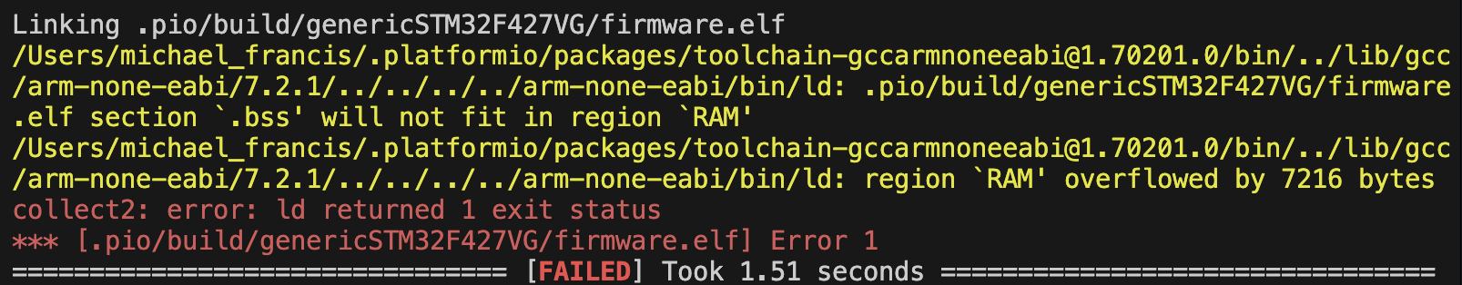
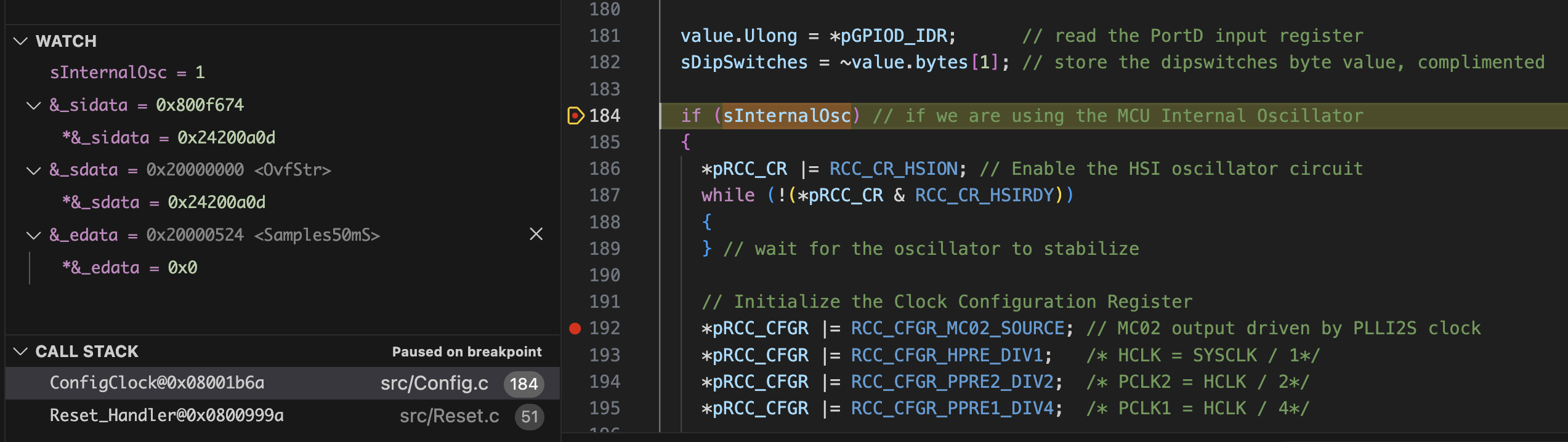
If your project doesn’t reach a breakpoint set in main(), that means it can actually only fail in a handful of places before. Very good for debugging.

The very first instruction that the processor executes should be the Reset_Handler. You can start the debugger at that very first instruction by setting a breakpoint there:

debug_init_break = break Reset_Handler

(docs) in the platformio.ini.

Which means execution should start in the startup_stm32f427xx.S startup file (I hope you have a startup assembly file in your project or your framework = ... provides it!), by standard

The startup file will initialize the stack pointer (sp), then immediately calls into SystemInit() to get the CPU clock pumped up to the maximum (usually via the PLL and a quartz oscillator), before continuing to copy the initial values for variables from flash to RAM, zeroing-out the uninitialized variables and buffers (.bss segment), initializing the C runtime library (call to __libc_init_array() and calling into the main() function.

See also the explanation of the startup file in:

As such, it can only fail in a handful of places, for example:

  • if the initial stack pointer (sp) is initialized wrongly, for example, to a address that can’t actually be written to, then the first push instruction will crash (as it attempts to push data onto a stack, aka at the stack pointer)
    • the initial SP is usually the highest address of RAM and the stack grows downwards (towards lower addresses)
  • clock initialization might fail, for example if the code is expecting a HSE / crystal oscillator to be connected, when there is none, or some macro definition is missing that causes the code to select the wrong clock source
  • while calling __libc_init_array() , it will also call all functions marked with attribute((constructor)) and C++ object constructors of globally allocated objects. If one of the constructor functions crashes, execution won’t get to main()

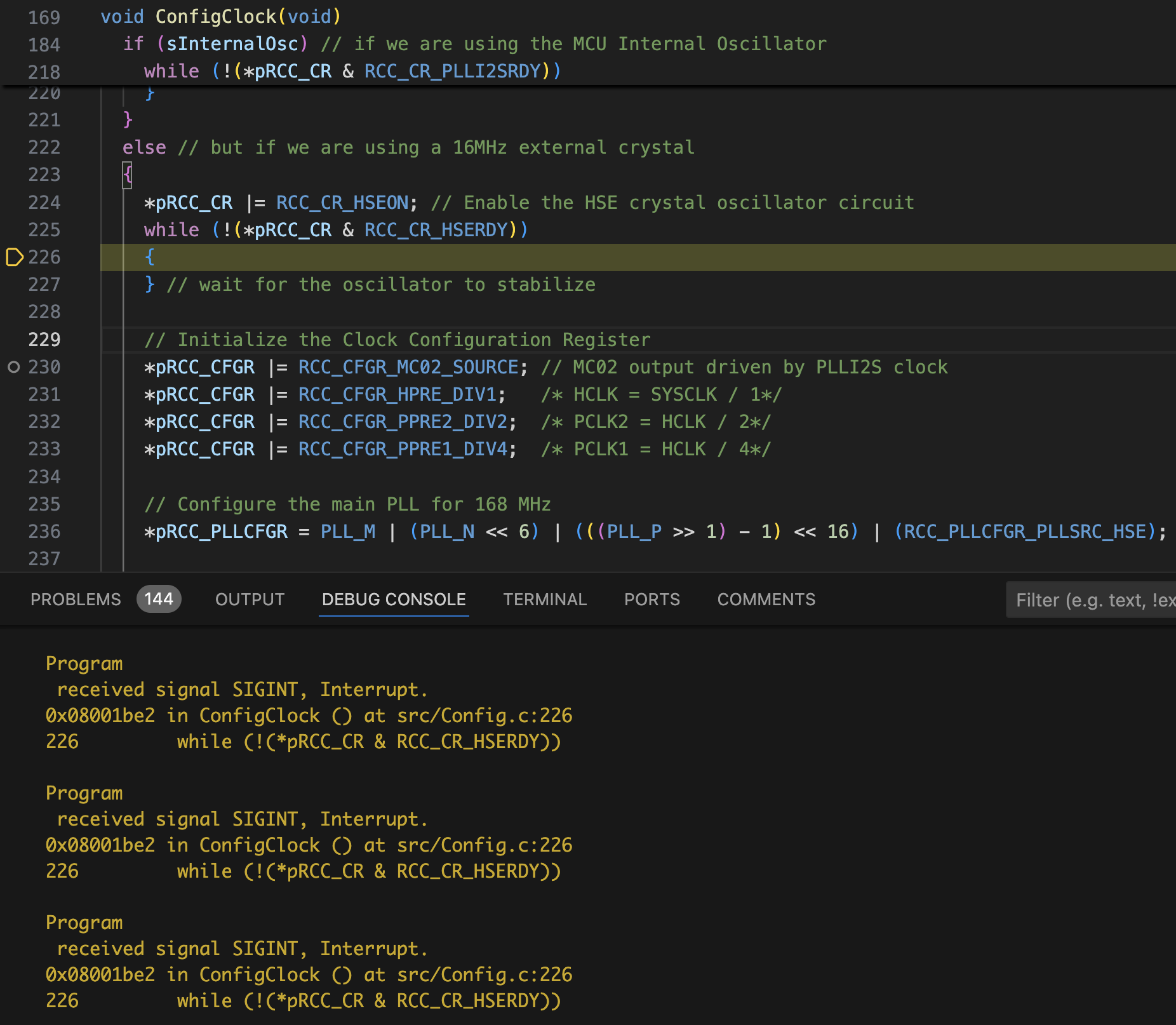
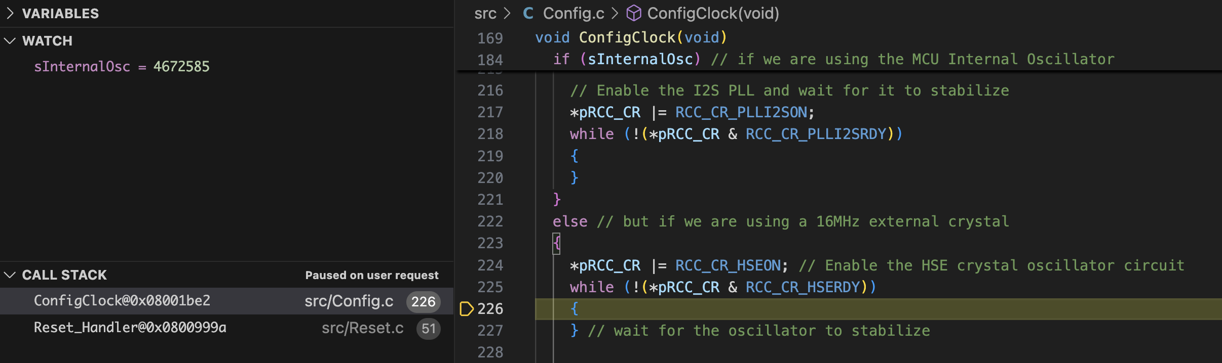
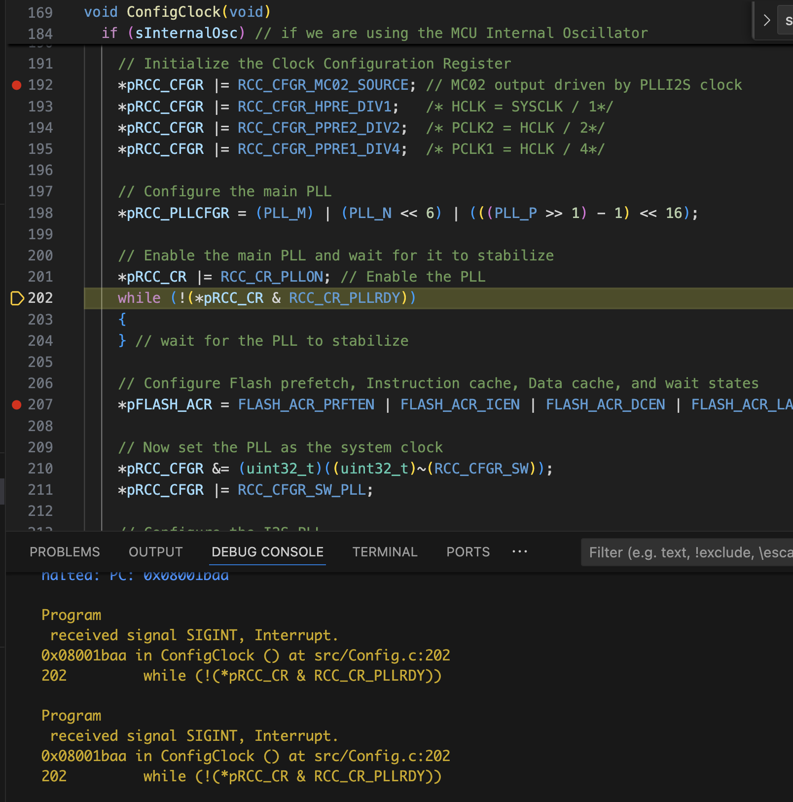
By stepping through the Reset_Handler’s assembly code line by line (and skipping over long copy or zeroing loops by setting a breakpoint and continuing), we could see exactly where it’s failing. We can also just let the program run (play button), then press the pause button to halt the processor. Then, one could see if the code is stuck in a loop it never exits, or if it has crashed and landed in the Hardfault_Handler() function. The “Call Stack” will then show the path that execution took to get to the crash, pin-pointing the problem.

But, to make a long story short, I already have a pretty good idea: There is actually a problem in the linker script numbers that I’ve posted. Looking back we settled on:

MEMORY
{
  CCMRAM    (xrw)    : ORIGIN = 0x10000000,   LENGTH = 64K
  RAM    (xrw)    : ORIGIN = 0x20000000,   LENGTH = 262144
  FLASH    (rx)    : ORIGIN = 0x8000000, LENGTH = 1048576
}

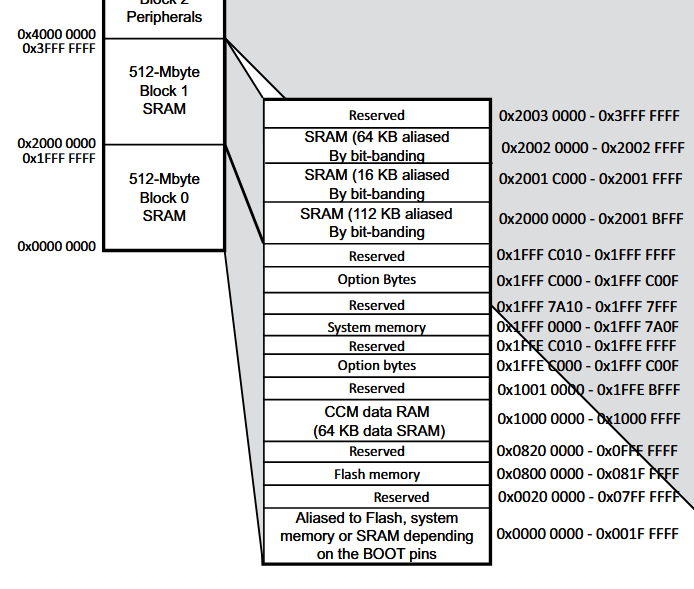
These RAM sizes are not correct here. By looking at the memory map of the STM32F427VG, we can see how much memory mapped is mapped to which addresses:

https://www.st.com/resource/en/datasheet/stm32f427vg.pdf, page 86

You can see the “256 KB” of RAM of the device are actually sitting in different blocks:

  • core-coupled-memory (CCM) is at 0x10000000 with a size of 64 kilobytes (good, exactly as we have it in the linker script)
  • the rest of the SRAM can be seen as one big continuous block starting at address 0x20000000 and of length 112 + 16 + 64 = 192 KB = 196608 bytes. Our linker script however says that there is 256 KB of RAM there. Wrong!!.
    • This will cause the linker script to set the stack pointer to “the end of RAM memory”, which is 0x20000000 + 256KB, at which there is no validly mapped memory, causing a hard crash (Hardfault_Handler()) when trying to access it.

Thus, we should instead write the MEMORY section as

MEMORY
{
  CCMRAM    (xrw)    : ORIGIN = 0x10000000,   LENGTH = 64K
  RAM       (xrw)    : ORIGIN = 0x20000000,   LENGTH = 192K
  FLASH      (rx)    : ORIGIN = 0x8000000,    LENGTH = 1024K
}

This also has the impliciation that, in order to use the 64K core-coupled-memory, we have to annotate variables that should live in that memory explicitly with a gcc attribute((section("..")) directive (see here), but I don’t think that’s relevant for now.

1 Like

Interesting… that was something I had noticed earlier today and wondered about, the fact that the RAM was in two separate ‘chunks’. After making the changes you suggested, the build failed with this:

I will look into this further… I’m pretty sure there’s a large chunk of memory allocated that I can reduce with no negative impact and at least that will get past this minor setback.

Thanks!

I set a breakpoint at the Reset_Handler. Here’s the code:

//    Reset.C

#include "PartnerE.h" //include sytem stack definitions

// Begin references to external globals
//
extern void *_estack; // initial stack-pointer address value (just above end of SRAM)
extern void *_sidata; // lowest address of initialized data in FLASH
extern void *_sdata;  // lowest address of initialized data copied to SRAM
extern void *_edata;  // address just above initialized data in SRAM (same as _sbss)
extern void *_sbss;	  // lowest address of uninitialized variables in SRAM
extern void *_ebss;	  // lowest address in free SRAM
//
// End references to external globals

// Begin function prototypes for called functions
//
void ConfigPower(void);		  // configure the power usage
void ConfigGPIO(void);		  // configure the GPIO port bits
void ConfigClock(void);		  // configure the Clock stuff
void __libc_init_array(void); // initialize the C runtime library stuff
int main(void);				  // main program function
//
// End function prototypes for called functions

// CPU hardware jumps here upon RESET
void __attribute__((naked, noreturn)) Reset_Handler()
{
	// NOTE: the following instruction allows starting up without a valid vector-table loaded
	// asm ("ldr sp, =_estack");							//load up a legal stack-pointer

	void **pSource, **pDest;														// copy all...
	for (pSource = &_sidata, pDest = &_sdata; pDest != &_edata; pSource++, pDest++) //...initialized data...
		*pDest = *pSource;															//...from FLASH to SRAM

	for (pDest = &_sbss; pDest != &_ebss; pDest++) // zero-fill the...
		*pDest = 0;								   //...uninitialized variables in SRAM

	// load known pattern into the entire system stack area
	register U32 *pStack; // pointer to the system stack

	for (pStack = (U32 *)&_ebss; pStack < (U32 *)&_estack; pStack++) // for each stack longword
	{
		*pStack = STACK_PATTERN32; // load it with the distinctive pattern
	}

	ConfigPower(); // power up everything we are gonna use

	ConfigGPIO(); // setup all GPIO port bits

	ConfigClock(); // setup all the clock stuff

	__libc_init_array(); // init the C runtime library stuff

	main(); // enter the main program code  [in PartnerE.c]

	for (;;) // endless loop
	{
		continue; // if "main" should ever return
	}
}

I stepped through and the call to ConfigClock() never returns. Here’s the configuration code module:

//    F:\BBRI\IMProCon\STM32\PartnerE\Config.c   12-Sep-15 11:44:13
//    ----------------------------------------

#include "Chip407.h"
#include "PartnerE.h"

// Begin definition of global variables
//
U32 sInternalOsc = 0; //"Using MCU Internal Oscillator" flag (0=no)
//
// End definition of global variables

// Begin references to external global variables
//
extern U8 sDipSwitches;          // DipSwitches byte
extern U32 *const pJumperUIO_BB; //"Use Internal Oscillator" jumper Bit-Band address

extern U32 *const pGPIOA_MODER;   // pointer to  Mode             Register
extern U32 *const pGPIOA_OTYPER;  // pointer to  Output Type      Register
extern U32 *const pGPIOA_OSPEEDR; // pointer to  Output Speed     Register
extern U32 *const pGPIOA_PUPDR;   // pointer to  PullUp/PullDown  Register
extern U32 *const pGPIOA_IDR;     // pointer to  Input  Data      Register
extern U32 *const pGPIOA_ODR;     // pointer to  Output Data      Register
extern U32 *const pGPIOA_BSRR;    // pointer to  Bit Set/Reset    Register
extern U32 *const pGPIOA_AFRL;    // pointer to  Alt Fun Low      Register
extern U32 *const pGPIOA_AFRH;    // pointer to  Alt Fun High     Register

extern U32 *const pGPIOB_MODER;   // pointer to  Mode             Register
extern U32 *const pGPIOB_OTYPER;  // pointer to  Output Type      Register
extern U32 *const pGPIOB_OSPEEDR; // pointer to  Output Speed     Register
extern U32 *const pGPIOB_PUPDR;   // pointer to  PullUp/PullDown  Register
extern U32 *const pGPIOB_IDR;     // pointer to  Input  Data      Register
extern U32 *const pGPIOB_ODR;     // pointer to  Output Data      Register
extern U32 *const pGPIOB_BSRR;    // pointer to  Bit Set/Reset    Register
extern U32 *const pGPIOB_AFRL;    // pointer to  Alt Fun Low      Register
extern U32 *const pGPIOB_AFRH;    // pointer to  Alt Fun High     Register

extern U32 *const pGPIOC_MODER;   // pointer to  Mode             Register
extern U32 *const pGPIOC_OTYPER;  // pointer to  Output Type      Register
extern U32 *const pGPIOC_OSPEEDR; // pointer to  Output Speed     Register
extern U32 *const pGPIOC_PUPDR;   // pointer to  PullUp/PullDown  Register
extern U32 *const pGPIOC_IDR;     // pointer to  Input  Data      Register
extern U32 *const pGPIOC_ODR;     // pointer to  Output Data      Register
extern U32 *const pGPIOC_BSRR;    // pointer to  Bit Set/Reset    Register
extern U32 *const pGPIOC_AFRL;    // pointer to  Alt Fun Low      Register
extern U32 *const pGPIOC_AFRH;    // pointer to  Alt Fun High     Register

extern U32 *const pGPIOD_MODER;   // pointer to  Mode             Register
extern U32 *const pGPIOD_OTYPER;  // pointer to  Output Type      Register
extern U32 *const pGPIOD_OSPEEDR; // pointer to  Output Speed     Register
extern U32 *const pGPIOD_PUPDR;   // pointer to  PullUp/PullDown  Register
extern U32 *const pGPIOD_IDR;     // pointer to  Input  Data      Register
extern U32 *const pGPIOD_ODR;     // pointer to  Output Data      Register
extern U32 *const pGPIOD_BSRR;    // pointer to  Bit Set/Reset    Register
extern U32 *const pGPIOD_AFRL;    // pointer to  Alt Fun Low      Register
extern U32 *const pGPIOD_AFRH;    // pointer to  Alt Fun High     Register

extern U32 *const pGPIOE_MODER;   // pointer to  Mode             Register
extern U32 *const pGPIOE_OTYPER;  // pointer to  Output Type      Register
extern U32 *const pGPIOE_OSPEEDR; // pointer to  Output Speed     Register
extern U32 *const pGPIOE_PUPDR;   // pointer to  PullUp/PullDown  Register
extern U32 *const pGPIOE_IDR;     // pointer to  Input  Data      Register
extern U32 *const pGPIOE_ODR;     // pointer to  Output Data      Register
extern U32 *const pGPIOE_BSRR;    // pointer to  Bit Set/Reset    Register
extern U32 *const pGPIOE_AFRL;    // pointer to  Alt Fun Low      Register
extern U32 *const pGPIOE_AFRH;    // pointer to  Alt Fun High     Register

extern U32 *const pRCC_CFGR;       // pointer to the RCC CFGR register
extern U32 *const pRCC_CR;         // pointer to the RCC CR register
extern U32 *const pRCC_APB1ENR;    // pointer to the RCC APB1ENR register
extern U32 *const pRCC_PLLCFGR;    // pointer to the RCC PLLCFGR register
extern U32 *const pRCC_PLLI2SCFGR; // pointer to the RCC PLLI2SCFGR register
extern U32 *const pFLASH_ACR;      // pointer to the FLASH ACR register
//
// End references to external global variables

void ConfigPower(void)
{
  VU32 *const pRCC_AHB1ENR = (VU32 *)(RCC_BASE + RCC_AHB1ENR_OFFSET); // create a pointer to register RCC_AHB1ENR
  VU32 *const pRCC_APB1ENR = (VU32 *)(RCC_BASE + RCC_APB1ENR_OFFSET); // create a pointer to register RCC_APB1ENR
  VU32 *const pRCC_APB2ENR = (VU32 *)(RCC_BASE + RCC_APB2ENR_OFFSET); // create a pointer to register RCC_APB2ENR
  VU32 *const pPWR_CR = (VU32 *)(PWR_BASE + PWR_CR_OFFSET);           // pointer to the PWR Control register

  *pRCC_AHB1ENR |= RCC_AHB1ENR_CCMDATARAMEN; // make sure the CCM SRAM clock is powered up
  *pRCC_AHB1ENR |= RCC_AHB1ENR_BKPSRAMEN;    // power the clock for the Backup SRAM
  *pRCC_AHB1ENR |= RCC_AHB1ENR_GPIOAEN;      // power the clock for GPIO Port A
  *pRCC_AHB1ENR |= RCC_AHB1ENR_GPIOBEN;      // power the clock for GPIO Port B
  *pRCC_AHB1ENR |= RCC_AHB1ENR_GPIOCEN;      // power the clock for GPIO Port C
  *pRCC_AHB1ENR |= RCC_AHB1ENR_GPIODEN;      // power the clock for GPIO Port D
  *pRCC_AHB1ENR |= RCC_AHB1ENR_GPIOEEN;      // power the clock for GPIO Port E
  *pRCC_AHB1ENR |= RCC_AHB1ENR_ETHMACEN;     // power the ethernet MAC clock
  *pRCC_AHB1ENR |= RCC_AHB1ENR_ETHMACTXEN;   // power the ethernet transmitter clock
  *pRCC_AHB1ENR |= RCC_AHB1ENR_ETHMACRXEN;   // power the ethernet receiver clock
  *pRCC_AHB1ENR |= RCC_AHB1ENR_ETHMACPTPEN;  // power the ethernet PTP clock ??? zzz

  *pRCC_APB1ENR |= RCC_APB1ENR_PWREN;    // Enable high performance mode (System frequency up to 168 MHz)
  *pRCC_APB1ENR |= RCC_APB1ENR_TIM7EN;   // power the clock for Timer7
  *pRCC_APB1ENR |= RCC_APB1ENR_TIM12EN;  // power the clock for Timer12
  *pRCC_APB1ENR |= RCC_APB1ENR_USART3EN; // power the clock for USART3  [PROG Logging]			[enc 13Feb22]
  *pRCC_APB1ENR |= RCC_APB1ENR_UART4EN;  // power the clock for USART4  [IRRISR]
  *pRCC_APB1ENR |= RCC_APB1ENR_I2C1EN;   // power the clock for I2C1    [EEPROM]

  *pRCC_APB2ENR |= RCC_APB2ENR_SYSCFGEN; // power the clock for the System Configuration Controller
  *pRCC_APB2ENR |= RCC_APB2ENR_USART1EN; // power the clock for USART1  [Logging]
  *pRCC_APB2ENR |= RCC_APB2ENR_USART6EN; // power the clock for USART6  [HMIISR]

  *pPWR_CR |= 0x000000F0; // enable power-loss detection at 2.9 volts
  *pPWR_CR |= 0x00000100; // disable startup write-protection for RTC & backup domain

  return; // return to caller
}

// Begin function ConfigGPIO
//
void ConfigGPIO(void) // declare myself, with no arguments
{
  *pGPIOA_MODER &= 0x3FFFFFFF;          // erase default JTAG JTDI signal at PA15
  *pGPIOA_MODER |= GPIOA_MODER_INI;     // Mode register Logical-OR initial value
  *pGPIOA_OTYPER |= GPIOA_OTYPER_INI;   // Output Type register Logical-OR initial value
  *pGPIOA_OSPEEDR |= GPIOA_OSPEEDR_INI; // Output Speed register Logical-OR initial value
  *pGPIOA_PUPDR |= GPIOA_PUPDR_INI;     // Pullup/Pulldown register Logical-OR initial value
  *pGPIOA_ODR |= GPIOA_ODR_INI;         // Output Data register Logical-OR initial value
  *pGPIOA_BSRR |= GPIOA_BSRR_INI;       // Bit Set/Reset register Logical-OR initial value
  *pGPIOA_AFRL |= GPIOA_AFRL_INI;       // Alternate Function Low register Logical-OR initial value
  *pGPIOA_AFRH |= GPIOA_AFRH_INI;       // Alternate Function High register Logical-OR initial value

  *pGPIOB_MODER = 0;                    //*** WIPE-OUT JTAG USAGE OF PORTB SO WE CAN USE SPI3 ***
  *pGPIOB_MODER |= GPIOB_MODER_INI;     // Mode register Logical-OR initial value
  *pGPIOB_OTYPER |= GPIOB_OTYPER_INI;   // Output Type register Logical-OR initial value
  *pGPIOB_OSPEEDR |= GPIOB_OSPEEDR_INI; // Output Speed register Logical-OR initial value
  *pGPIOB_PUPDR |= GPIOB_PUPDR_INI;     // Pullup/Pulldown register Logical-OR initial value
  *pGPIOB_ODR |= GPIOB_ODR_INI;         // Output Data register Logical-OR initial value
  *pGPIOB_BSRR |= GPIOB_BSRR_INI;       // Bit Set/Reset register Logical-OR initial value
  *pGPIOB_AFRL |= GPIOB_AFRL_INI;       // Alternate Function Low register Logical-OR initial value
  *pGPIOB_AFRH |= GPIOB_AFRH_INI;       // Alternate Function High register Logical-OR initial value

  *pGPIOC_MODER |= GPIOC_MODER_INI;     // Mode register Logical-OR initial value
  *pGPIOC_OTYPER |= GPIOC_OTYPER_INI;   // Output Type register Logical-OR initial value
  *pGPIOC_OSPEEDR |= GPIOC_OSPEEDR_INI; // Output Speed register Logical-OR initial value
  *pGPIOC_PUPDR |= GPIOC_PUPDR_INI;     // Pullup/Pulldown register Logical-OR initial value
  *pGPIOC_ODR |= GPIOC_ODR_INI;         // Output Data register Logical-OR initial value
  *pGPIOC_BSRR |= GPIOC_BSRR_INI;       // Bit Set/Reset register Logical-OR initial value
  *pGPIOC_AFRL |= GPIOC_AFRL_INI;       // Alternate Function Low register Logical-OR initial value
  *pGPIOC_AFRH |= GPIOC_AFRH_INI;       // Alternate Function High register Logical-OR initial value

  *pGPIOD_MODER |= GPIOD_MODER_INI;     // Mode register Logical-OR initial value
  *pGPIOD_OTYPER |= GPIOD_OTYPER_INI;   // Output Type register Logical-OR initial value
  *pGPIOD_OSPEEDR |= GPIOD_OSPEEDR_INI; // Output Speed register Logical-OR initial value
  *pGPIOD_PUPDR |= GPIOD_PUPDR_INI;     // Pullup/Pulldown register Logical-OR initial value
  *pGPIOD_ODR |= GPIOD_ODR_INI;         // Output Data register Logical-OR initial value
  *pGPIOD_BSRR |= GPIOD_BSRR_INI;       // Bit Set/Reset register Logical-OR initial value
  *pGPIOD_AFRL |= GPIOD_AFRL_INI;       // Alternate Function Low register Logical-OR initial value
  *pGPIOD_AFRH |= GPIOD_AFRH_INI;       // Alternate Function High register Logical-OR initial value

  *pGPIOE_MODER |= GPIOE_MODER_INI;     // Mode register Logical-OR initial value
  *pGPIOE_OTYPER |= GPIOE_OTYPER_INI;   // Output Type register Logical-OR initial value
  *pGPIOE_OSPEEDR |= GPIOE_OSPEEDR_INI; // Output Speed register Logical-OR initial value
  *pGPIOE_PUPDR |= GPIOE_PUPDR_INI;     // Pullup/Pulldown register Logical-OR initial value
  *pGPIOE_ODR |= GPIOE_ODR_INI;         // Output Data register Logical-OR initial value
  *pGPIOE_BSRR |= GPIOE_BSRR_INI;       // Bit Set/Reset register Logical-OR initial value
  *pGPIOE_AFRL |= GPIOE_AFRL_INI;       // Alternate Function Low register Logical-OR initial value
  *pGPIOE_AFRH |= GPIOE_AFRH_INI;       // Alternate Function High register Logical-OR initial value

  return; // return to caller
}
//
// End function ConfigGPIO

void ConfigClock(void)
{

  union // create a union of...
  {
    U8 bytes[4];  // four bytes
    U16 Uword[2]; // two U16
    S16 Sword[2]; // two S16
    U32 Ulong;    // one U32
    S32 Slong;    // one S32
  } value;        //... and give it a name

  value.Ulong = *pGPIOD_IDR;      // read the PortD input register
  sDipSwitches = ~value.bytes[1]; // store the dipswitches byte value, complimented

  if (sInternalOsc) // if we are using the MCU Internal Oscillator
  {
    *pRCC_CR |= RCC_CR_HSION; // Enable the HSI oscillator circuit
    while (!(*pRCC_CR & RCC_CR_HSIRDY))
    {
    } // wait for the oscillator to stabilize

    // Initialize the Clock Configuration Register
    *pRCC_CFGR |= RCC_CFGR_MC02_SOURCE; // MC02 output driven by PLLI2S clock
    *pRCC_CFGR |= RCC_CFGR_HPRE_DIV1;   /* HCLK = SYSCLK / 1*/
    *pRCC_CFGR |= RCC_CFGR_PPRE2_DIV2;  /* PCLK2 = HCLK / 2*/
    *pRCC_CFGR |= RCC_CFGR_PPRE1_DIV4;  /* PCLK1 = HCLK / 4*/

    // Configure the main PLL
    *pRCC_PLLCFGR = (PLL_M) | (PLL_N << 6) | (((PLL_P >> 1) - 1) << 16);

    // Enable the main PLL and wait for it to stabilize
    *pRCC_CR |= RCC_CR_PLLON; // Enable the PLL
    while (!(*pRCC_CR & RCC_CR_PLLRDY))
    {
    } // wait for the PLL to stabilize

    // Configure Flash prefetch, Instruction cache, Data cache, and wait states
    *pFLASH_ACR = FLASH_ACR_PRFTEN | FLASH_ACR_ICEN | FLASH_ACR_DCEN | FLASH_ACR_LATENCY_5WS; //[ENC 13Feb20]

    // Now set the PLL as the system clock
    *pRCC_CFGR &= (uint32_t)((uint32_t)~(RCC_CFGR_SW));
    *pRCC_CFGR |= RCC_CFGR_SW_PLL;

    // Configure the I2S PLL
    *pRCC_PLLI2SCFGR = (2 << 28) | (100 << 6);

    // Enable the I2S PLL and wait for it to stabilize
    *pRCC_CR |= RCC_CR_PLLI2SON;
    while (!(*pRCC_CR & RCC_CR_PLLI2SRDY))
    {
    }
  }
  else // but if we are using a 16MHz external crystal
  {
    *pRCC_CR |= RCC_CR_HSEON; // Enable the HSE crystal oscillator circuit
    while (!(*pRCC_CR & RCC_CR_HSERDY))
    {
    } // wait for the oscillator to stabilize

    // Initialize the Clock Configuration Register
    *pRCC_CFGR |= RCC_CFGR_MC02_SOURCE; // MC02 output driven by PLLI2S clock
    *pRCC_CFGR |= RCC_CFGR_HPRE_DIV1;   /* HCLK = SYSCLK / 1*/
    *pRCC_CFGR |= RCC_CFGR_PPRE2_DIV2;  /* PCLK2 = HCLK / 2*/
    *pRCC_CFGR |= RCC_CFGR_PPRE1_DIV4;  /* PCLK1 = HCLK / 4*/

    // Configure the main PLL for 168 MHz
    *pRCC_PLLCFGR = PLL_M | (PLL_N << 6) | (((PLL_P >> 1) - 1) << 16) | (RCC_PLLCFGR_PLLSRC_HSE);

    // Enable the Over-drive to extend the clock frequency to 180 Mhz  [NEVER INVESTIGATED!!!]
    // PWR->CR |= PWR_CR_ODEN;
    // while((PWR->CSR & PWR_CSR_ODRDY) == 0) {};
    // PWR->CR |= PWR_CR_ODSWEN;
    // while((PWR->CSR & PWR_CSR_ODSWRDY) == 0) {};

    // Enable the main PLL and wait for it to stabilize
    *pRCC_CR |= RCC_CR_PLLON; // Enable the PLL
    while (!(*pRCC_CR & RCC_CR_PLLRDY))
    {
    } // wait for the PLL to stabilize

    // Configure Flash prefetch, Instruction cache, Data cache, and wait states
    *pFLASH_ACR = FLASH_ACR_PRFTEN | FLASH_ACR_ICEN | FLASH_ACR_DCEN | FLASH_ACR_LATENCY_5WS; //[ENC 13Feb20]

    // Now set the PLL as the system clock
    *pRCC_CFGR &= (uint32_t)((uint32_t)~(RCC_CFGR_SW));
    *pRCC_CFGR |= RCC_CFGR_SW_PLL;

    // Configure the I2S PLL
    *pRCC_PLLI2SCFGR = (2 << 28) | (100 << 6);

    // Enable the I2S PLL and wait for it to stabilize
    *pRCC_CR |= RCC_CR_PLLI2SON;
    while (!(*pRCC_CR & RCC_CR_PLLI2SRDY))
    {
    }
  }
  return; // return to caller
}

It hangs on line 232:

*pRCC_CFGR |= RCC_CFGR_HPRE_DIV1;   /* HCLK = SYSCLK / 1*/

Here’s the output from the debug console as I repeatedly clicked on ‘Run’, waited a few seconds, and then clicked on ‘Pause’:


Program
 received signal SIGINT, Interrupt.
0x08001be2 in ConfigClock () at src/Config.c:232
232	   *pRCC_CR |= RCC_CR_HSEON;			  //Enable the HSE crystal oscillator circuit

Program
 received signal SIGINT, Interrupt.
0x08001be2 in ConfigClock () at src/Config.c:232
232	   *pRCC_CR |= RCC_CR_HSEON;			  //Enable the HSE crystal oscillator circuit

Program
 received signal SIGINT, Interrupt.
0x08001be2 in ConfigClock () at src/Config.c:232
232	   *pRCC_CR |= RCC_CR_HSEON;			  //Enable the HSE crystal oscillator circuit

So now I’m looking for info on SIGINT.

When you set this variable to 1, does it boot up?

No, the oscillator apparently never stabilizes:

Hm, this is strange… the value of sInternalOsc:

When sInternalOsc is set to zero, it is equal to zero when line 184 executes, but if set to 1, it is equal to 4672585? o_O

At that point, if sInternalOsc does not have the correct starting value that you set in the code, then the copy loop failed to copy the initial value of the variables from Flash to RAM.

In the debugger, you can add a watch for the expressions

&_sidata
&_sdata
&_edata

to the see what start and end address is being used for the copy from Flash to RAM loop.

Ultimately, these values and especially the difference &_edata - &_sdata should not be zero (it should have something to copy).

This is getting more exciting by the minute! :^D

I had the debug option set to this, somehow:
image

Adjusted that, and now I get this:

…and now the PLL never stabilizes: