i just want to say what a wonderful community this is!
i am grateful for the assistance and feedback
thank you! and for enabling me to comment further
i am so happy that there is a potential fix to this self inflicted issue!
i could have of course just purchased another skr… but i am stubborn
i am into electronics but am lacking experience with this particular software/hardware.
unfortunately the mofset on my wanhao duplicator í3 plus burnt itself out!
as such was unable to heat the hotbed! it rendered the printer unusable
(i have purchased an external mosfet board to prevent the fire hazard!)
so… i decided to upgrade to 32 bit. only to break the board before i even uploaded the modified firmware!! i didn’t look into where it would be housed in the printer frame
and whilst trying to find a place for it - i rendered the board disabled!
i anticipate i will be asking more questions when i get my board up and running
i am new to pio (it is a great tool) and just updating and customising the firmware etc was initially a steep learning curve. (i had previously edited the marlin files in Microsoft visual studio)
i modified marlin to be compatible with the printer i have been using
but was unable to upload it due to the missing sd-card!!
it is highly embarasing and frustrating to say the least!
i was unable to find the solution online and stumbled on the post here which encouraged me to join the community.
Seriously!, I just want to express my gratitude.
I am overwhelmed by the support you have both shown.
You have gone way beyond… what i imagined would result from my questions…the time and effort you both (as a group) have put in is really amazing… for the reverse engineering
thankful is an understatement. i would have been stranded without your input
i will try to make good to the best of my severely limited capabilities
and apply the input you so kindly provided
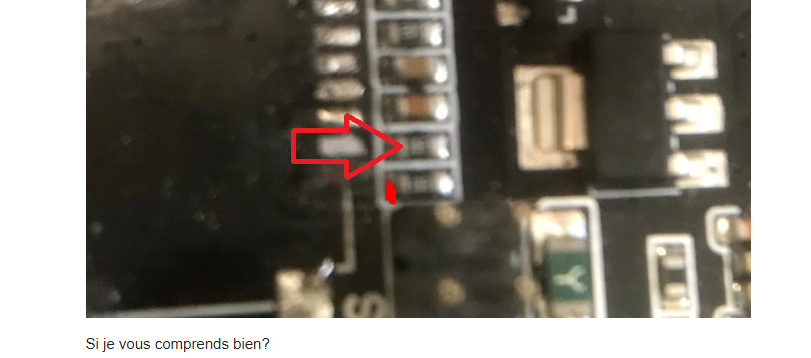
Quote
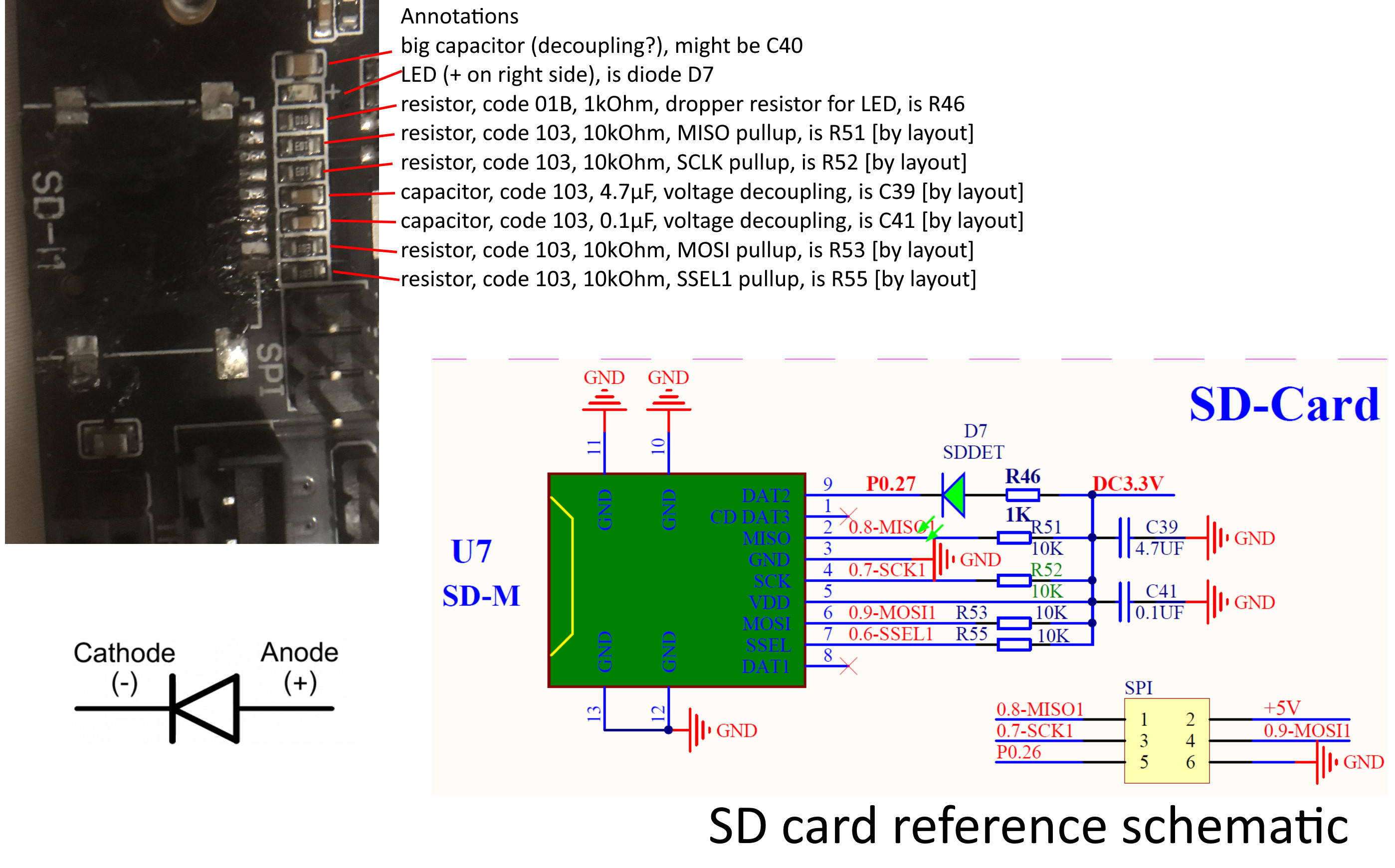
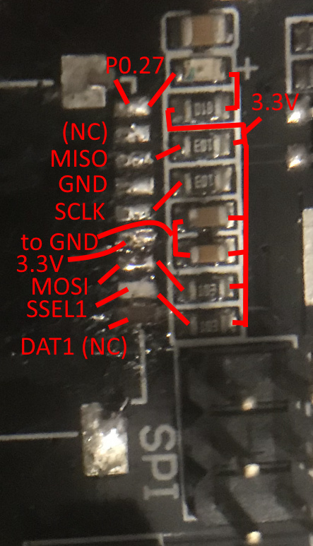
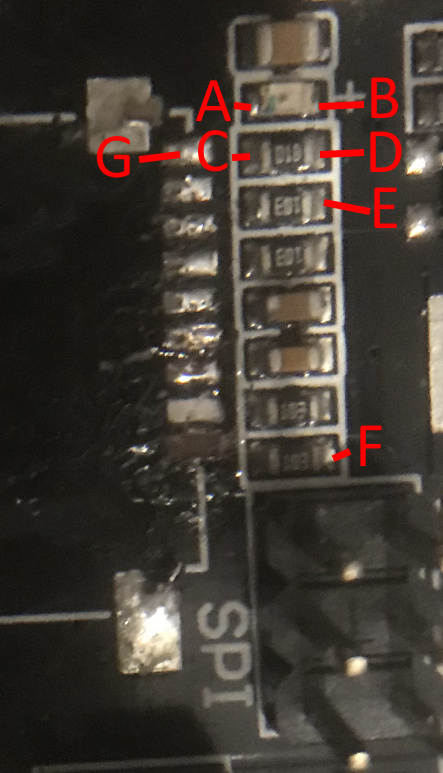
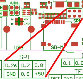
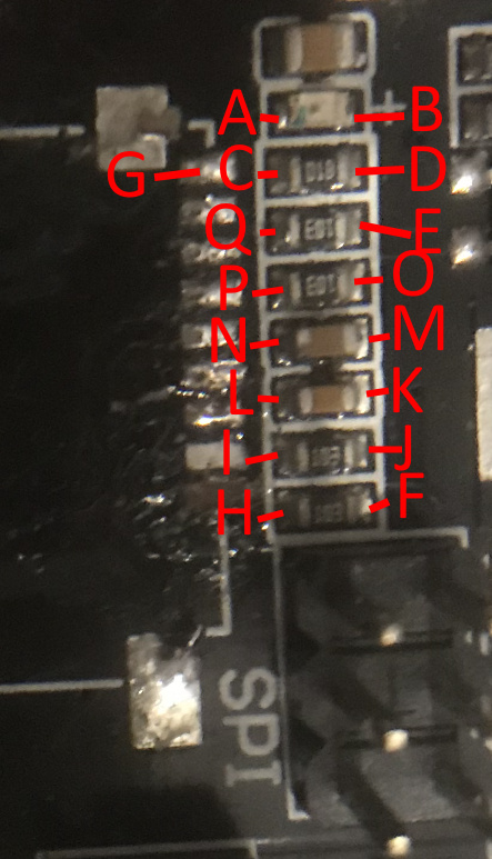
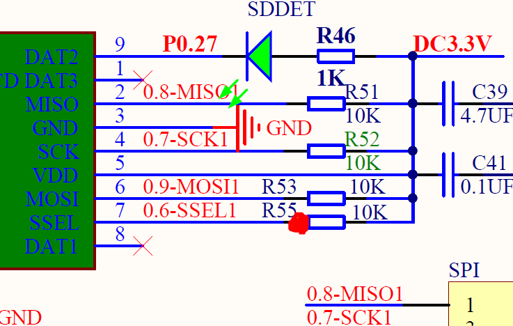
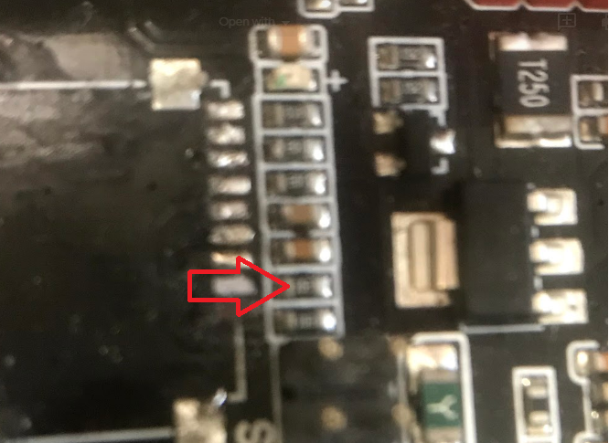
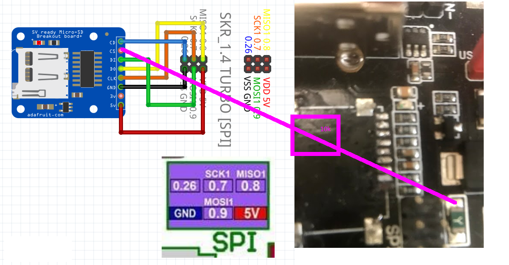
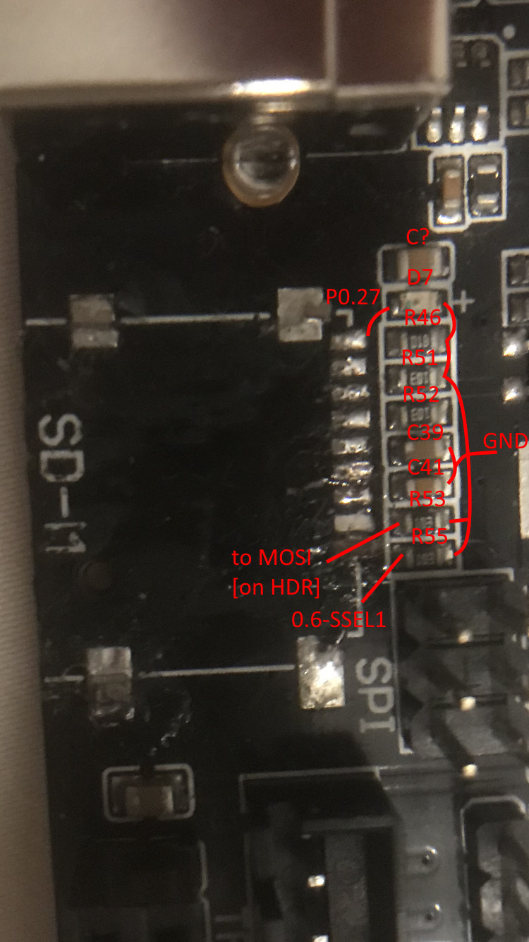
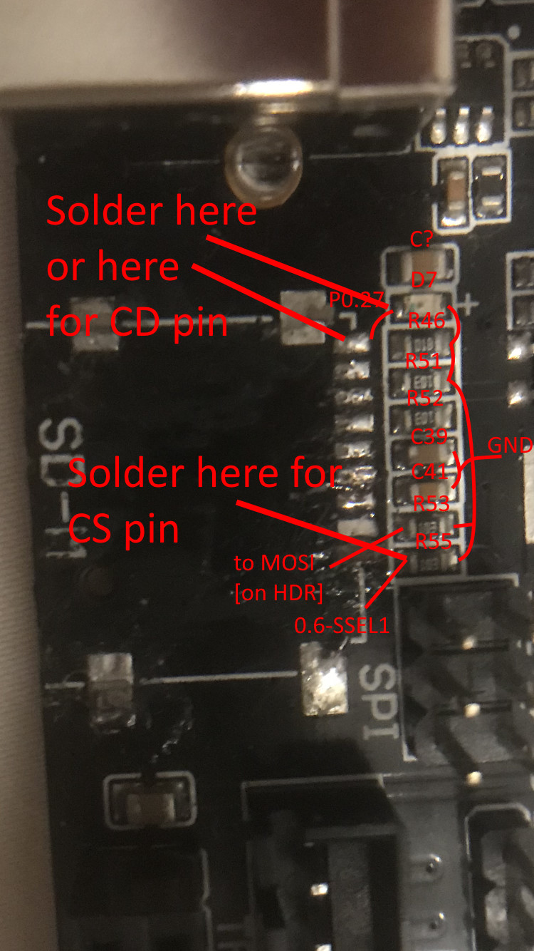
Which would mean that the 2 wires need to be solderer to the left side of the first resistor (P0.27) and last resistor (SSEL1) of the column.
sadly both of the pads (DAT1[8] & SSEL [7] have been damaged
so i cannot solder those connections on skr 1.4 turbo [SD-M]
i think it is unlikely i will be able to solder wires to the smd resistor terminals.
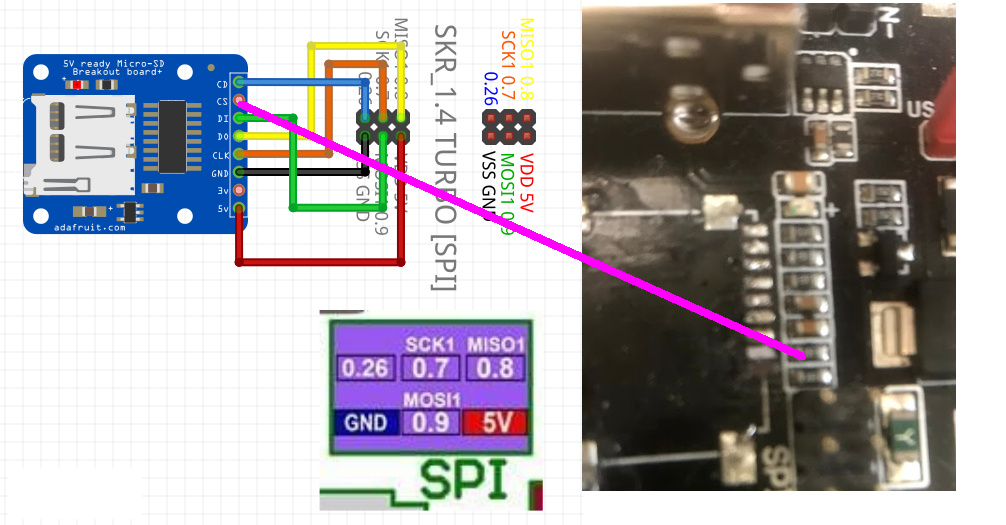
Hm both sides of the resistor shouldn’t go through the to the 0.8-MOSI header. I’m deducing from the I and J connections that the left side of the resistor must go the header (and must also be connected to the SD card SPI signals). So this is what we get from the known tested connections
So the solder points are clear after all, to the left of D7 and to the left of R55.
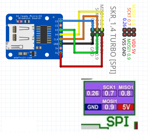
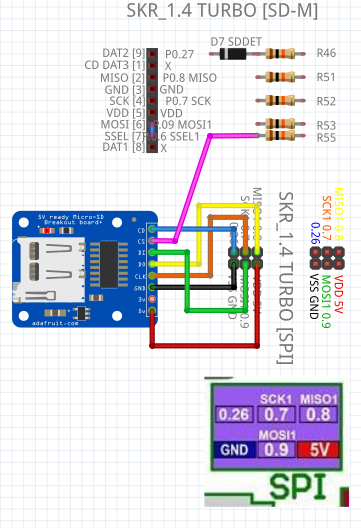
In this diagram, CD should be solderer to the left of Diode D7, becuase the bootloader will use pin P0.27 which is connected to the original SD card holder; P0.26 on the SPI header is a different pin. Of course, there is a chance that this pin might also be ignored by the bootloader – only way to be sure it to test it with and without that connection. All other connections are correct.
Hm I personally would not use hot air. You would also need kapton tape to isolate the plastic headers (e.g. SPI) so that they don’t melt. Really, a soldering iron with a small tip is good enough. You will need some practice of course and the right technique. For example, you should add solder to the left side of the resistor (or diode) and also to one end of the wire first (“pre-tinning”). Then just bring the pre-tinned components together, touch both of them with the fine soldering iron to melt them, then back off.