hi,
i need some help in configuring my ini file so that i can load code to a custom atmega328p stand alone chip via an FTDI.
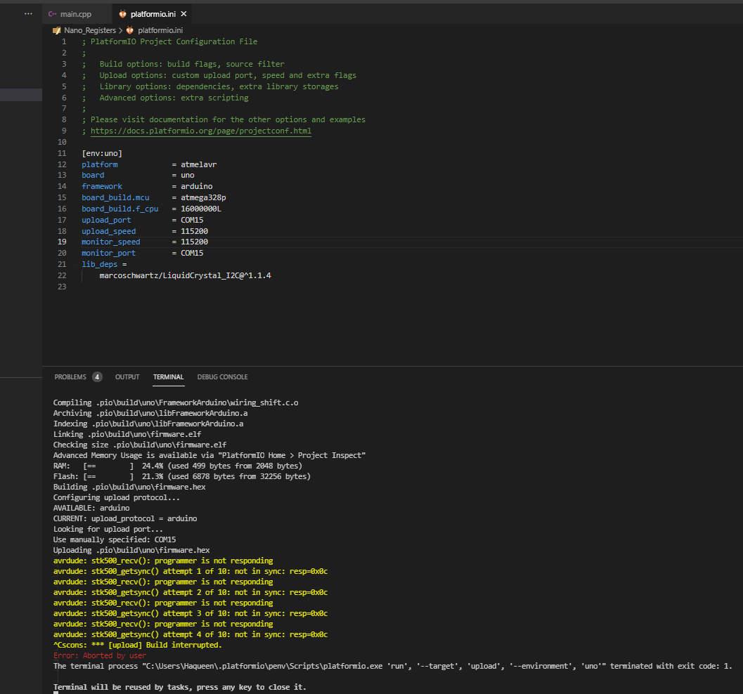
Here is how my file looks like.
i wired the DTR to 100nF capacitor which is connected to a resistor the to the reset pin. The other end of the resistor is connected to the 5v source that is coming from the FTDI.
Yes i tried baudrates 1200, 2400, 4800, 19200, 38400, 57600, and 115200 . but couldnt get a positive result. I haven’t bother with 9600
The RX of the adapter goes correctly to the TX of the chip, and vice versa?
What about the crystal, does the chip have one? When the bootlaoder was programmed, they also set the fuses to something, so the chip may need an external clock now.
Your previous uno configuration should work just fine, it’s clearly an issue in either the wiring, the crystal, or the bootloader being wrong (either in content or in fuses).
If you can’t spot an error per above, I recommend building an ISP programmer using an Uno and setting it up accordingly. (Though if the fuses tell it to a crystal and there is none, you need to unbrick it by providing the clock).
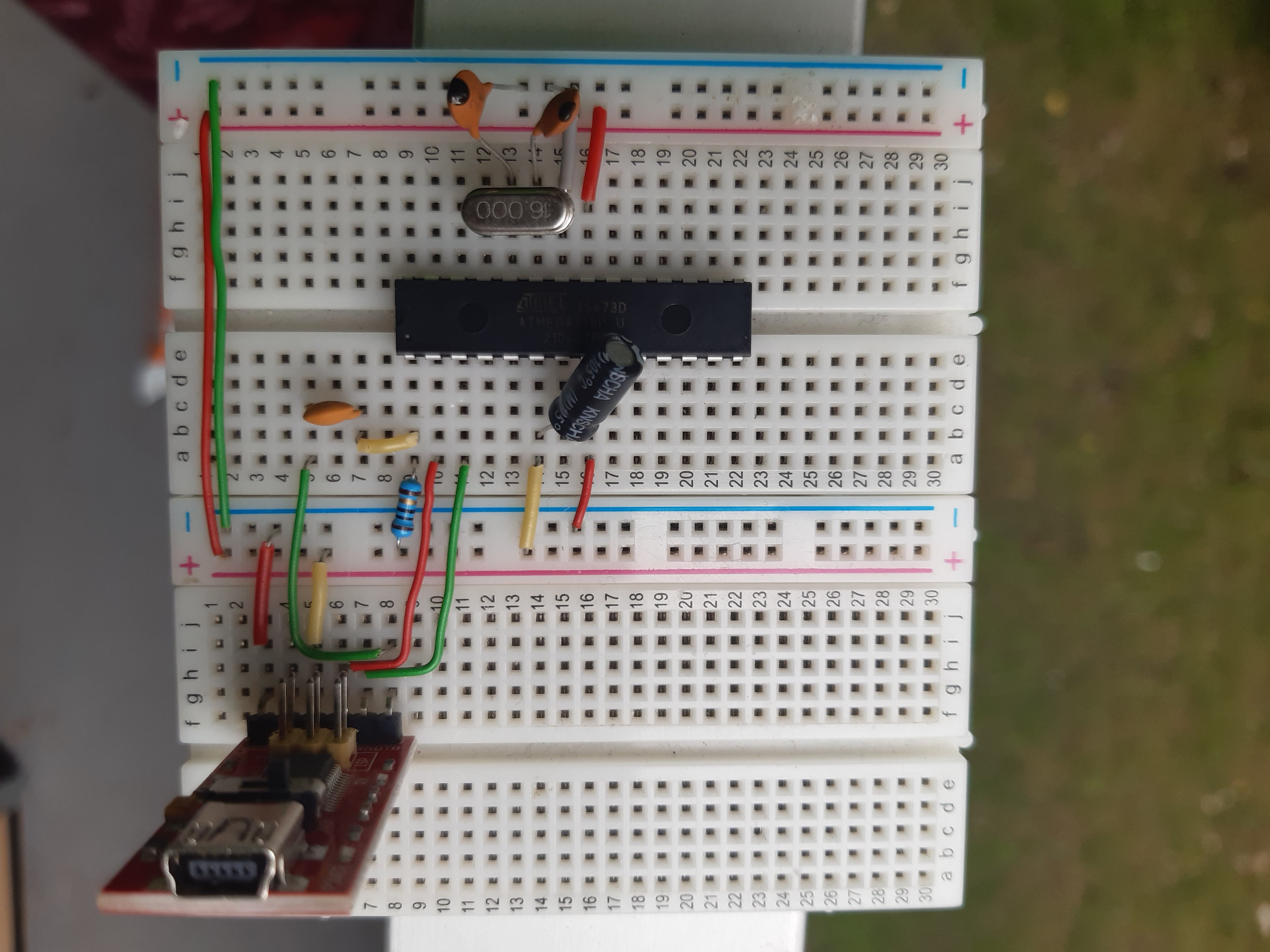
If so, your wiring is “all over the shop” I’m afraid. The Atmega328P has no GND connection as your GND rail is connected to DTS and the 5V rail looks to be connected to TXD on the FTDI chip. (Maybe your list of connections is back to front?)
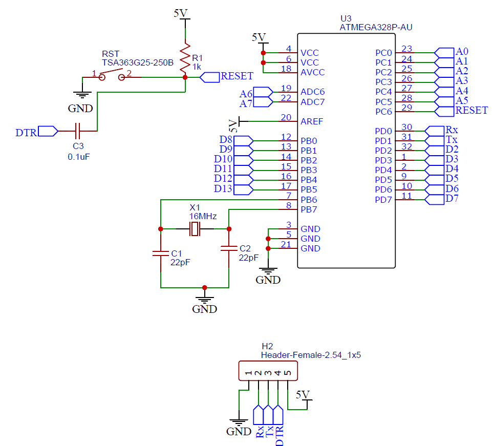
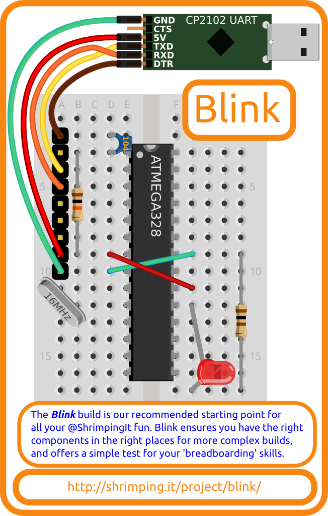
What markings are on the two capacitors connected to the crystal/ They should be 22 pF (marked 22) The remaining three capacitors should be marked 104 (100 nF).
I just magnified the picture. The rightmost pin seems to be DTR, then you can decipher XD, so probably RXD. In other words, the order of pins is just mirrored.
The wiring to Pin 1 (RESET) is OK. Also RX and TX are wired OK. But then it seems to be the case that the wiring is upside-down (i.e., pin 1 is assumed to be at F22). The XTAL needs to be on the lower half (pin 9 and 10), e.g., C17 and C18. Vcc should be pin 7, e.g. A15, and GND pin 8, e.g. A16 (already there). Now adjust the Vcc and GND on the upper half. Vcc to pin 20, e.g., I17, and GND pin 22, e.g. I15 (already there).
Now you should have blocking caps between the Vcc and GND pins on the upper and lower half. Use ceramic 100nF, not a 10µF as in the photo. Finally, the resistor value looks funny. brown-black-black-gold is 10Ω in my book. It should 10kΩ.