Hi All.
I have been working a project building a “semi-smartwatch” based on esp32 for a little over a year. I am new to electronics, programming and pcb design so I love this new hobby. At any rate, I finished my pcb design and got some prototypes made. Everything seems to be working as expected. However, one of the top priorities in my design considerations was battery life (it uses a 3.7V lipo battery). However, my first prototype used a 150 mAh battery and only lasted about 3-4 days . So that would make my current draw something like 1.5 - 2 miliamps. I was expecting to get at least twice that based on simply the information from the data sheets of all the major components that went into the design. Of course there are going to be leakages and losses in things like pullup/down resistors etc. but I am not familiar with what some of the major loss mechanisms are nor how to address them. I was hoping someone here could give me some pointers. I would be happy to start by posting my schematic, discussing my code, and posting details of my pcb design (just don’t laugh at me for being a noob).
Oh, I mentioned the Nordic Power Profiler Kit 2. I saw this thing in some forums and thought I would give it a try since I am concerned about my power draw - and it is really a nice piece of work! It is extremely easy to use and works great (no I am not sponsored by them)! You can find a description here but it basically tells you how much current is being used by your device. It is really made for low power applications (uA-1A).
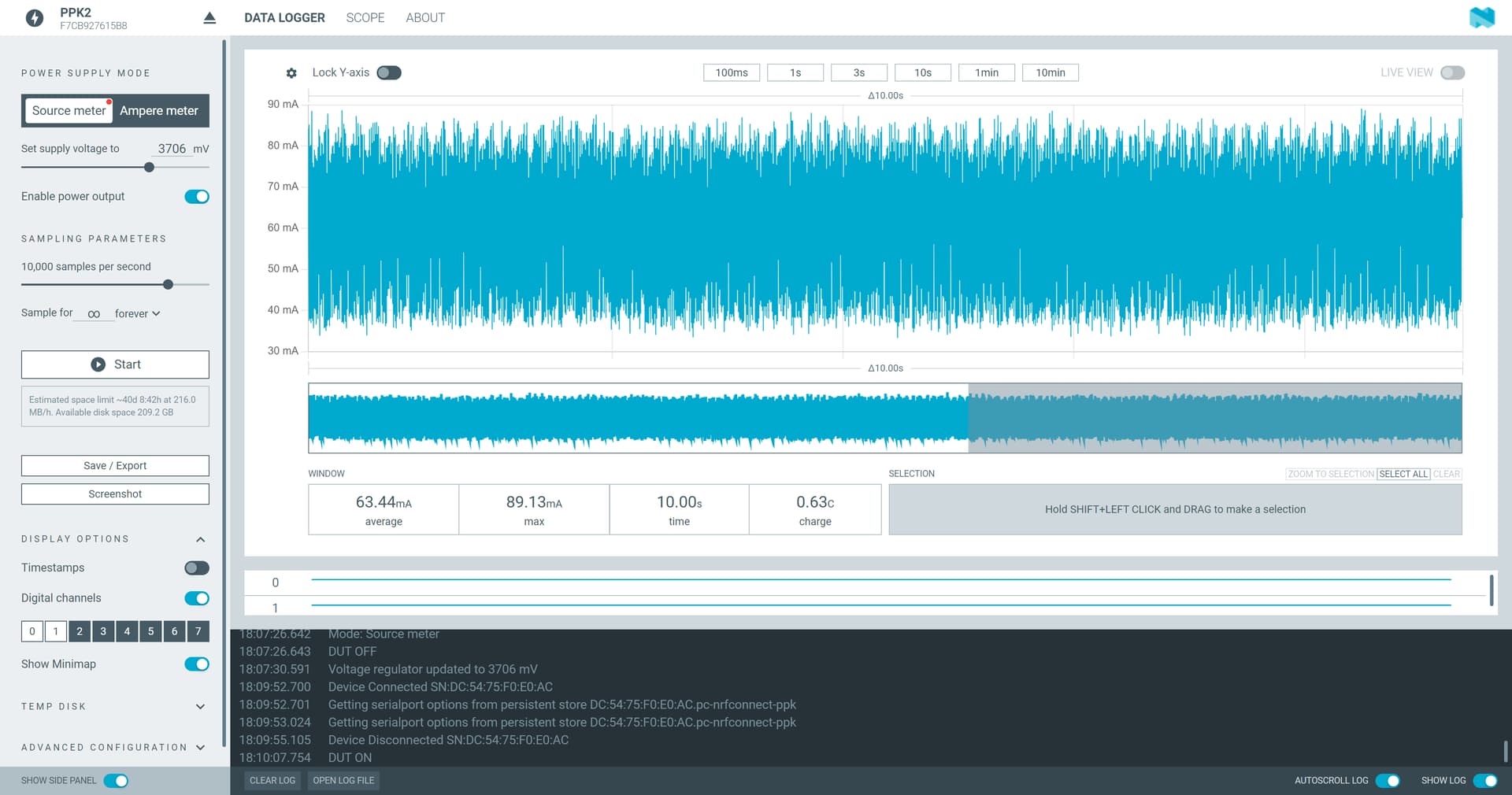
So when I first fired it up on my digital watch with everything running (esp32-S3, DS3231 Real-time clock, BMI-270 motion sensor, MAX17048 fuel gauge ic, SH-1106 oled display) I was seeing a current draw of about 63 mA
since battery life was a key design parameter, I put the esp32 in deep sleep for most of the time. Here you can see it transition to deep sleep:
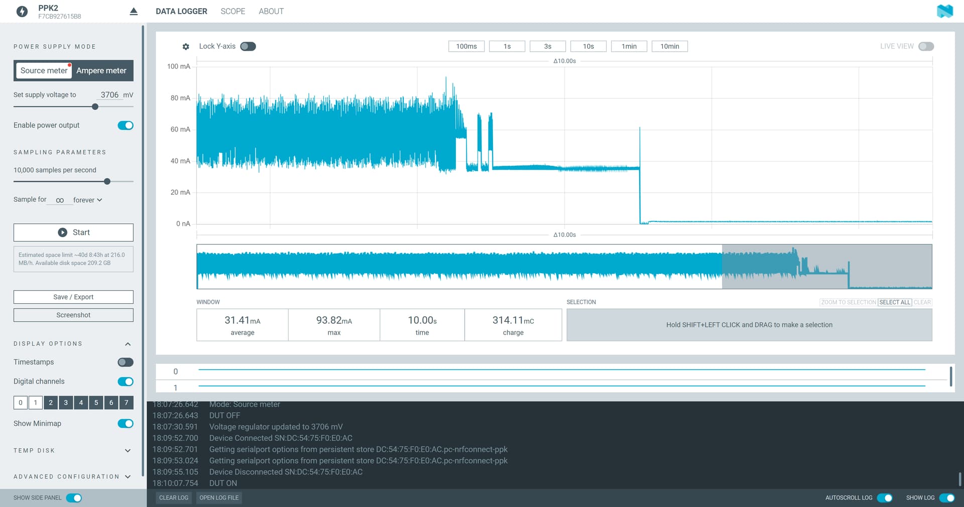
As I mentioned before, since it lasted about 3-4 days being in deep sleep most of the time, I expected a current draw to be 1.5mA to 2mA while in deep sleep and PPK2 showed that was spot on at 1.5mA!
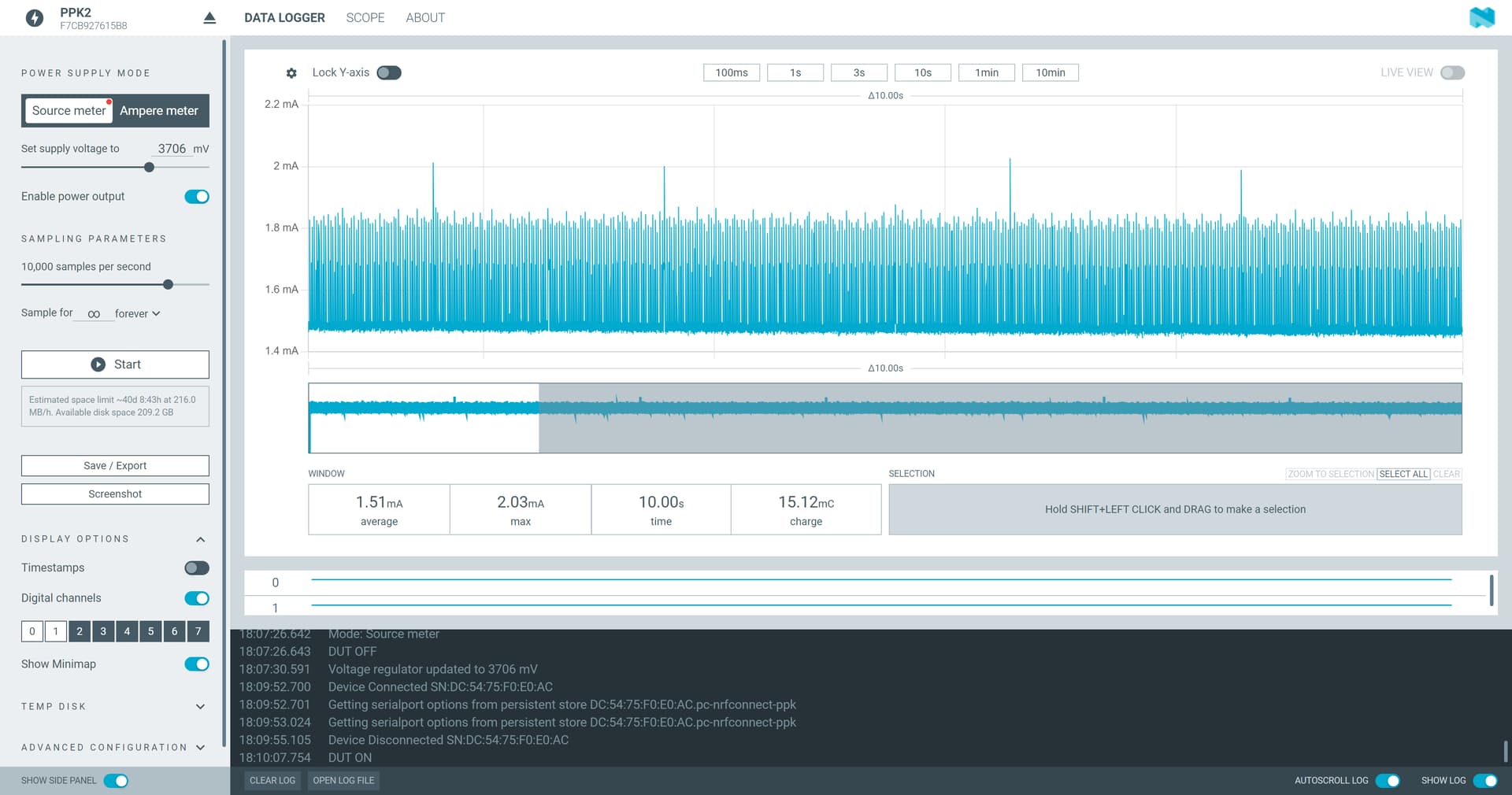
Another cool thing is I have a piezo buzzer that beeps everytime I hit a button on the watch and you can see the “pulses” of each button press
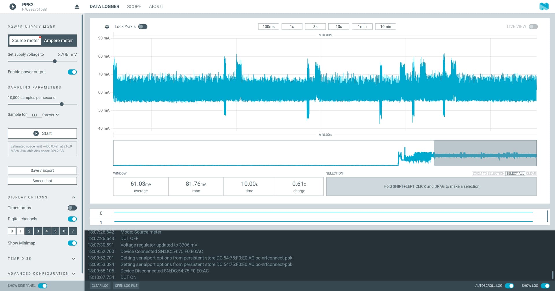
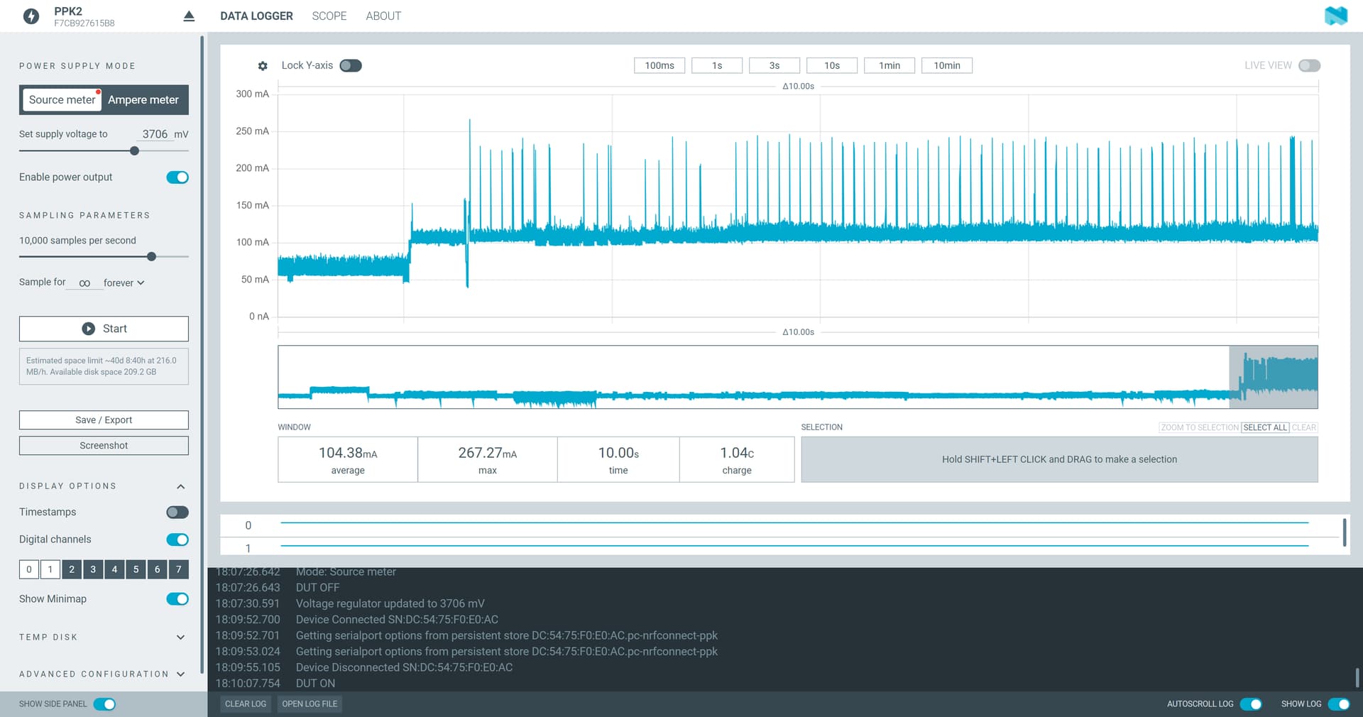
The watch is “semi-smart” since it can use the esp32 to set itself using Wi-Fi and getting the time from an NTP server. Talk about power consumption! This is what using WiFi looks like, but I dont know what those spikes are.
Anyway, I thought this was waaay cool so I wanted to share it with you guys and ask again if I could get some pointers on how to reduce the power consumption. If I could cut it in half i.e. get the “deep-sleep” state down to about 0.7 mA I would be ecstatic! I already have an idea that I think would help. The DS3231 RTC chip has a coin cell battery “backup” and when running off of that instead of the LiPo it uses significantly less power. However, I still have it running of the main 3.7V lipo even while sleeping. I was wondering if I could created a +3.3V “power bus” that all modules except the esp32 will be connected to. If I use something like a p-channel mosfet as a switch (one of the esp32 gpio connected to the gate) then I could only have these components “powered” when the esp32 wakes up from deep sleep. I think that may help but that could cause other start-up problem.
Anyway, thanks for listening. Any help is really appreciated!
Fish